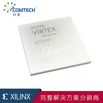
• Overview
  • Specification
  • Technical documentation

VIRTEX-VU product advantages

Virtex® UltraScale™ devices provide the best performance and integration at 20nm, including serial I/O bandwidth and logic capacity. As the only high-end FPGA in the industry at the 20nm process node, this series is suitable for applications ranging from 400G networks to large-scale ASIC prototyping/simulation.

value Advantage
Programmable system integration
  • Up to 5.5M system logic unit, using 20nm process, and 2nd generation 3D IC
  • Integrated 100G Ethernet MAC and 150G Interlaken core
Improved system performance
  • High utilization rate increases the speed by two levels
  • 30G Transceiver: 28G backplane for chip-to-chip and chip-to-fiber
  • 16G backplane transceiver with half power consumption
  • 2400Mb/s DDR4 can work stably under different PVT conditions
BOM cost reduction
  • Cost reduction by up to 50% – ½ of the cost per port of the Nx100G system
  • The integration of VCXO and fPLL (frequency-divided phase-locked loop) can reduce the cost of clock components
  • Mid-range speed grade chip can support 2400 Mb/s DDR4
Total power consumption reduction
  • Up to 40% lower power consumption compared to the previous generation
  • Realize fine-grained clock gating function through an ASIC-like clock
  • Enhanced system logic unit packaging reduces dynamic power consumption
Accelerate design productivity
  • Pin compatible with Kintex® UltraScale devices, high scalability
  • Seamless pin migration from 20nm plane to 16nm FinFET
  • Co-optimize with Vivado® Design Suite to accelerate design closure

VIRTEX-VU product list

    • Model
    • Logic Unit
    • DSP Slice
    • Memory (Kb)
    • GTH 16.3 Gb/s transceiver
    • GTY 30.5 Gb/s transceiver
    • Maximum number of I/O pins
    • XCVU160
    • 2027
    • 1560
    • 115.2
    • 52
    • 52
    • 702
    • XCVU190
    • 2350
    • 1800
    • 132.9
    • 60
    • 60
    • 702